Long ago I promised my friend Nick a mod for a guitar pedal of his. His 8-bit fuzz pedal caused a volume drop that he couldn’t overcome by tweaking the settings, and he didn’t want to put a boost after because he would have to hit two pedals every time he wanted to switch to his fuzz. I had been looking at making a couple of different boost circuits and offered to put one in his pedal.
Now, some years later, I’m actually putting some effort into the project. The circuit I chose is the Mosfet Booster pedal from AMZ . The circuit was simple and would make for a very transparent gain stage. The idea is to make a small add-on board for his current pedal and wire the boost in line before the output jack.
I had seen a Hack-a-Day series about creating PCB’s in a number of different software, in particular a walk-through of using Eagle CAD. I’ve seen so many mentions of Eagle CAD over the years, but never used it. This simple circuit would make a good intro to the program.
Step one was to install Eagle and get some additional libraries set up (AdaFruit’s and Sparkfun’s Libraries).
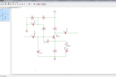
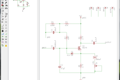
Once I had the software set up I laid out the schematic, doing my best to navigate the libraries and find the right components. Laying out the schematic was very straightforward overall, I just need to learn some keyboard shortcuts and I’ll be on my way.
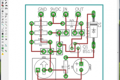
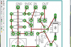
With the schematic created I then generated a board and started laying out the components and traces. I will be doing the first board on some 4mm X 6mm double-sided PCB proto-boards. I kept that in mind as I laid the traces. I like to fold over the excess lead material on the components and use them to make all of the connections.
Eagle’s board editor is possibly my favorite tool I’ve found recently. . I have always taken my circuits to a protoboard, then spent a lot of time laying out the parts and hoping I had all of the connections correct. Eagle links all the components to make sure you don’t miss any connections, and can automatically reroute as you drag components around. PCB design just got so much more approachable.
I spent a good amount of time tweaking the layout of everything I had put in. I got an initial revision done, but realized that I had no connections for power or IO on the board. After a few minutes on Google I was able to add the pads into the schematic and to link and the associated traces. When I went back to the board, I had my IO pads.
I positioned these on the edge of the board so that all of wires would be connected at the same point so the board would be manageable once it was built. I plan to use some screw terminals with the right spacing for the PCB I’m going to use.
The parts have been sitting on my work desk for a month or two at this point, so the board shouldn’t be far off. Construction should be much easier than my boards with the past now that I have this point-to-point-ish layout to reference.


